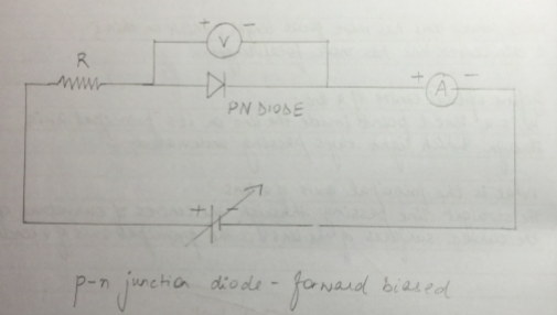
p n junction circuit diagram
PN Junction | Notes For Engineering Electronics Device and Circuits. 16 Images about PN Junction | Notes For Engineering Electronics Device and Circuits : What is the formation of PN-Junction? - Polytechnic Hub, To Draw The I-V Characteristic Curve For P-N Junction In Forward Bias and also Energy-band diagram of a silicon p-n junction solar cell (Reproduced.
PN Junction | Notes For Engineering Electronics Device And Circuits
 www.notesforengineering.com
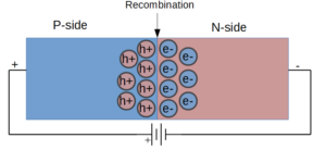
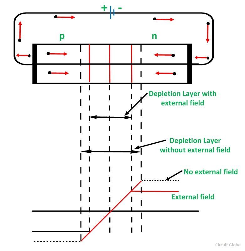
junction pn biased reverse type applied potential said then positive negative
Pn Junction Connection By Circuit Diagram In Forward Biased. - YouTube
 www.youtube.com
junction pn circuit connection biased diagram forward
PPT - CMOS Circuit Design, Layout And Simulation PowerPoint
 www.slideserve.com
voltage junction pn cmos simulation circuit layout
CBSE Biology Practical Class XII - Drawing I-V Characteristics Graph Of
 notesforfree.com
diode biasing resistance cbse xii siimusti
Energy-band Diagram For The Metal-semiconductor Junction (Schottky
 www.researchgate.net
semiconductor junction schottky
P-N Junction - Electronics Reference
 electronicsreference.com
junction terminal
Junction Field Effect Transistor Or JFET Tutorial
 www.electronics-tutorials.ws
transistor effect junction field electronics jfet symbol symbols circuit basics diagram jfets transistors knowledge construction circuits fields configurations shown basic
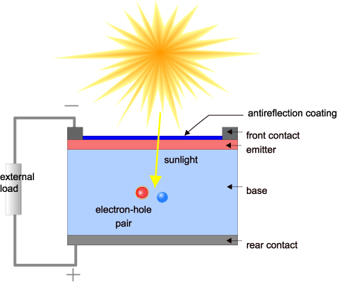
Solar Cell Structure | PVEducation
 www.pveducation.org
solar cell pv structure cells operation works pveducation photovoltaic panel junction energy devices basic conversion cross section applications components graphene
Miirbe: Forward Bias Pn Junction Diode Diagram
 miribelleg.blogspot.com
pn diode zener siimusti miirbe
What Is Forward Bias P N Junction? - Circuit Globe
 circuitglobe.com
bias
Energy-band Diagram Of A Silicon P-n Junction Solar Cell (Reproduced
 www.researchgate.net
reproduced
If We Short Circuit The Terminals Of A P-n Junction, Why Isn't There A
Difference Between NPN & PNP Transistor With Comparison Chart - Circuit
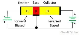 circuitglobe.com
npn transistor pnp circuit difference between diagram definition
To Draw The I-V Characteristic Curve For P-N Junction In Forward Bias
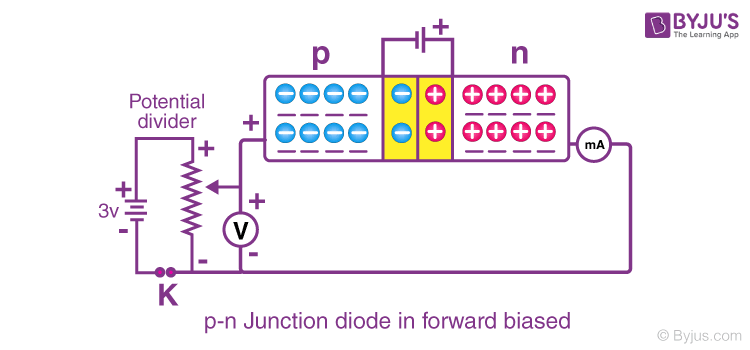 byjus.com
characteristic diode biased
NanoHUB.org - Resources: ECE 606 Lecture 20: Electrostatics Of P-N
 nanohub.org
junction nanohub diodes electrostatics lecture
What Is The Formation Of PN-Junction? - Polytechnic Hub
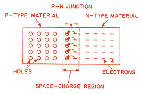 www.polytechnichub.com
junction pn formation
Junction field effect transistor or jfet tutorial. Npn transistor pnp circuit difference between diagram definition. Nanohub.org